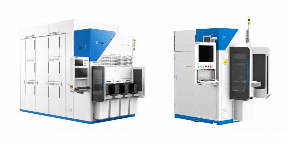
Single Wafer Cleaner
본문
It is a single etching and cleaning equipment using chemical, UPW and physical method on wafer surfaces.
Feature
- 1. 1Xnm level process capability
- 2. Compact desigh & high throughput
- 3. Contamination control technology
- 4. High end Material
- 5. Green Factory Technology
- 6. Multi Process Nozzle configuration
- 7. High stability & reliability
- 8. Easy Maintenance Design
- 9. SEMI Standard, CE Mark
Application
- - Semiconductor, OLEDoS, LED Process, R&D
- - Pre/Post Clean(DHF, SC1, Spray, IPA Dry)
- - Backside Clean(Front & Backside Megasonic)
- - Backside strip(Poly Decap, Bevel Etch)