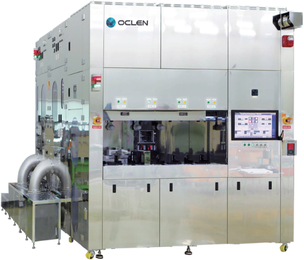
Metal Lift Off
본문
It removes a metal layer and photo-resist on a sapphire wafer used in a LED process through physical/chemical method.

Feature
- 1. Wafer auto conveyance by index robot and transfer robot
- 2. Minimize metal contamination
- 3. Able to collect metal of wafer
- 4. Energy saving mode
- 5. Compact equipment (Minimize footprint)
Application
- - LED process, 100mm (4"), 200mm (8")


